


Dedicated to Semiconductor and Precision Optical Equipment: High-Precision CNC-Machined Aluminum Alloy Substrates / Carrier Plates
Hongsinn-978
Unlock precision in semiconductor & optical manufacturing with our custom CNC machined aluminum pedestals. High flatness, hard anodized, cleanroom ready. Perfect for wafer carriers & vacuum chambers. Get a quote.
Delivery
FOB
minimum order
1 piece
Supply Ability
5000piece / Week
Country of Origin
Shenzhen
Stock Time
7~15Day
Quantity:
US $0.59 - US $10.68 / piece
Custom Aluminum Semiconductor Pedestals | CNC Machined for Perfection Upgrade your equipment with our hard-anodized machined pedestals. Superior flatness ±0.01mm, strict location tolerance, vacuum-ready (Type III Anodized). ISO certified QC. Perfect for wafer carriers & optical bases. Get a quick quote now!
Product Overview
This is a core precision structural substrate specifically designed for semiconductor manufacturing equipment, precision optical instruments, and vacuum chambers. Fabricated from high-strength aluminum alloy, this component undergoes a complex, multi-stage process involving precision milling and drilling on a vertical CNC machining center.
This is a core precision structural substrate specifically designed for semiconductor manufacturing equipment, precision optical instruments, and vacuum chambers. Fabricated from high-strength aluminum alloy, this component undergoes a complex, multi-stage process involving precision milling and drilling on a vertical CNC machining center.
Its intricate hole pattern layout, extremely stringent flatness requirements, and rigorous hard anodized surface finish make it an ideal choice for applications such as wafer carriers, sensor positioning mounts, heating pedestals, or optical path platforms. We offer fully customized services—ranging from single-unit prototyping to mass production—to meet your exact tolerance specifications.
Core Product Features
To achieve higher rankings in search results, we translate our product's technical specifications into tangible customer benefits:
Rigorous Geometric Tolerances and Flatness
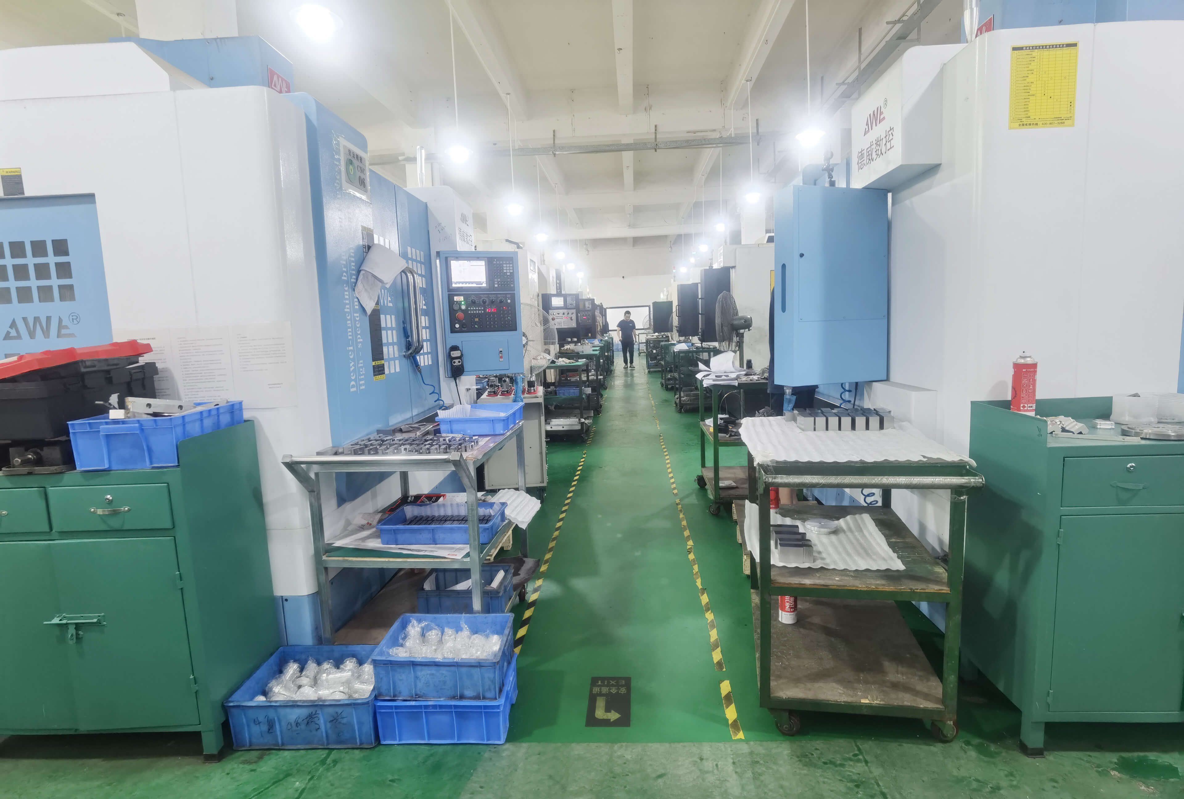
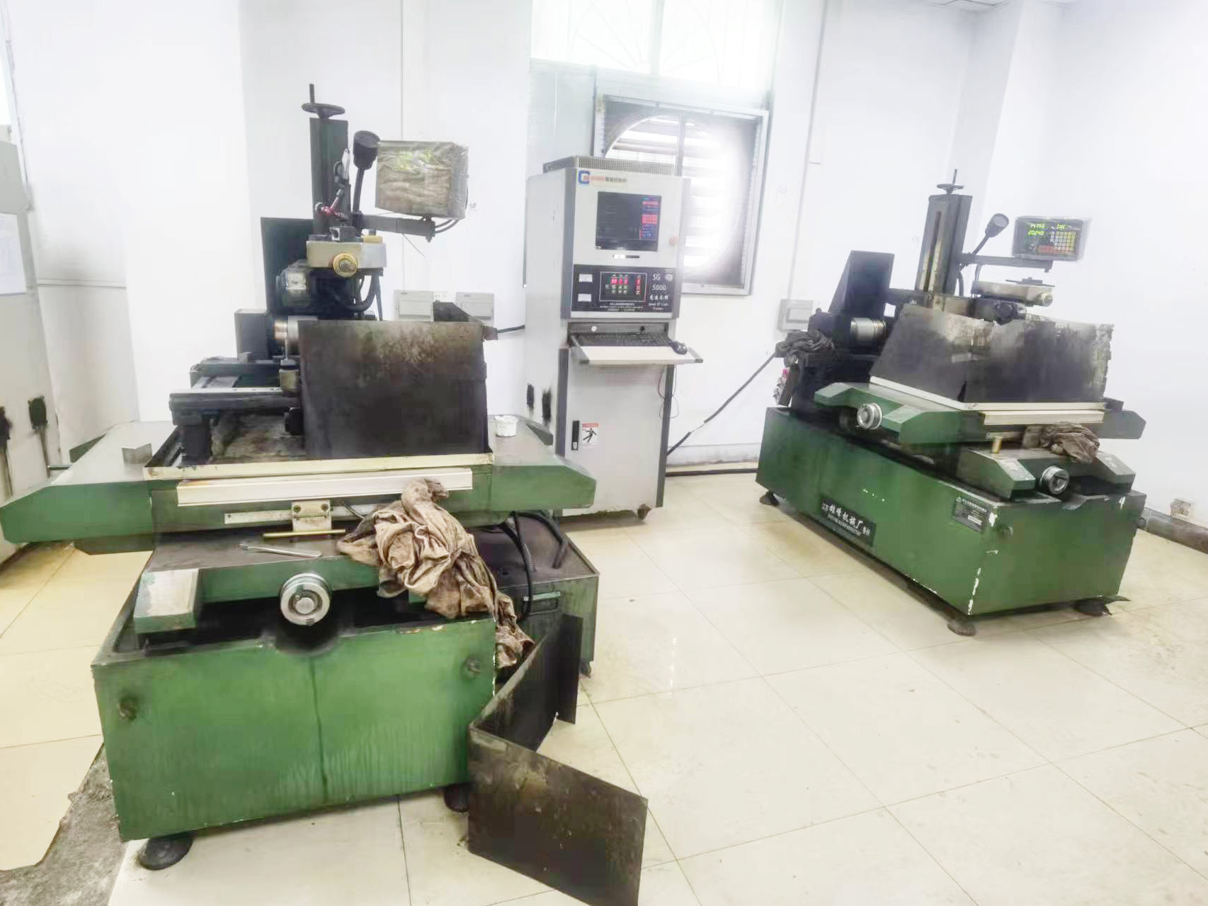
The semiconductor and optics industries demand exceptionally high precision. Utilizing state-of-the-art CNC machining equipment and rigorous aging treatment processes, we maintain the flatness of large-diameter discs within ±0.01mm (depending on specific dimensions), ensuring the precise alignment of wafers or optical components during subsequent processing stages.
The semiconductor and optics industries demand exceptionally high precision. Utilizing state-of-the-art CNC machining equipment and rigorous aging treatment processes, we maintain the flatness of large-diameter discs within ±0.01mm (depending on specific dimensions), ensuring the precise alignment of wafers or optical components during subsequent processing stages.
Complex, Fully Automated Hole Layouts
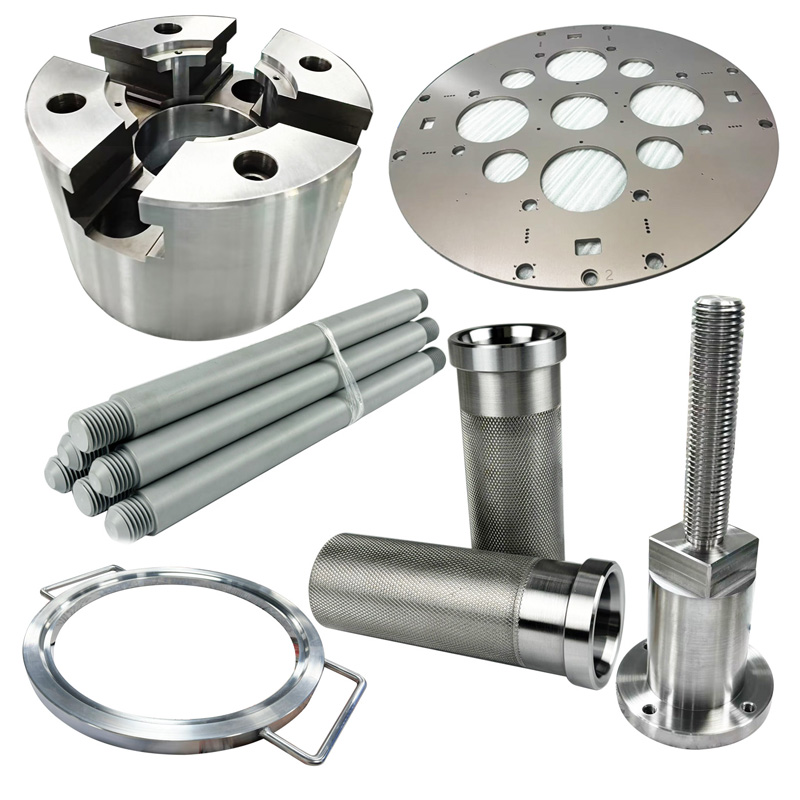
The disc surface features a uniform distribution of various hole types—including countersunk holes, dowel pin holes, through-holes, and custom-shaped recesses (such as rectangular slots)—specifically designed for mounting precision sensors, vacuum pneumatic components, heating elements, or robotic arm interfaces. The positional tolerance of every hole is verified via 100% inspection using a Coordinate Measuring Machine (CMM).
The disc surface features a uniform distribution of various hole types—including countersunk holes, dowel pin holes, through-holes, and custom-shaped recesses (such as rectangular slots)—specifically designed for mounting precision sensors, vacuum pneumatic components, heating elements, or robotic arm interfaces. The positional tolerance of every hole is verified via 100% inspection using a Coordinate Measuring Machine (CMM).
Hard Anodizing (Type III) Suitable for Cleanroom Environments
The surface of the components undergoes a hard anodizing treatment (resulting in a gray-brown finish). This process not only imparts exceptional surface hardness and wear resistance but, more importantly, ensures extremely low"outgassing"characteristics in vacuum or high-temperature environments. Furthermore, it provides electrical insulation and corrosion resistance, fully complying with the operational standards required for semiconductor cleanrooms.
The surface of the components undergoes a hard anodizing treatment (resulting in a gray-brown finish). This process not only imparts exceptional surface hardness and wear resistance but, more importantly, ensures extremely low"outgassing"characteristics in vacuum or high-temperature environments. Furthermore, it provides electrical insulation and corrosion resistance, fully complying with the operational standards required for semiconductor cleanrooms.
Customized Traceability and Marking
The crisp, clearly defined"No. 2"engraving (or QR code/serial number) serves as a key indicator of our industrialized management and traceability capabilities. Regardless of the number of workstations required for your equipment, we guarantee the uniqueness of every component, thereby facilitating ease of installation and maintenance.
The crisp, clearly defined"No. 2"engraving (or QR code/serial number) serves as a key indicator of our industrialized management and traceability capabilities. Regardless of the number of workstations required for your equipment, we guarantee the uniqueness of every component, thereby facilitating ease of installation and maintenance.
|
Industry Applications
This precision CNC-machined substrate serves as a robust foundation for core equipment across the following industries:
This precision CNC-machined substrate serves as a robust foundation for core equipment across the following industries:
Semiconductor Equipment: Used as the wafer-bearing pedestal (or chuck) within etching and deposition (CVD/PVD) chambers.
Precision Optics & Laser Systems: Used to support large mirrors and lenses, or serving as a multi-aperture positioning platform for laser beam path systems.
Vacuum Coating Equipment: Serves as the rotating turntable substrate for multi-station turret systems.
Automated Inspection Equipment: Functions as a precision carrier fixture for lithium-ion battery or display panel production lines.
Why Choose Our Semiconductor-Grade Machining Services?
Focus on Ultra-Precision Machining: We fully understand the exacting demands placed on every micron of tolerance within the semiconductor and optics industries.
Focus on Ultra-Precision Machining: We fully understand the exacting demands placed on every micron of tolerance within the semiconductor and optics industries.
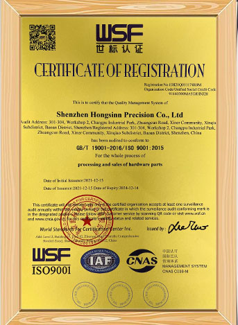
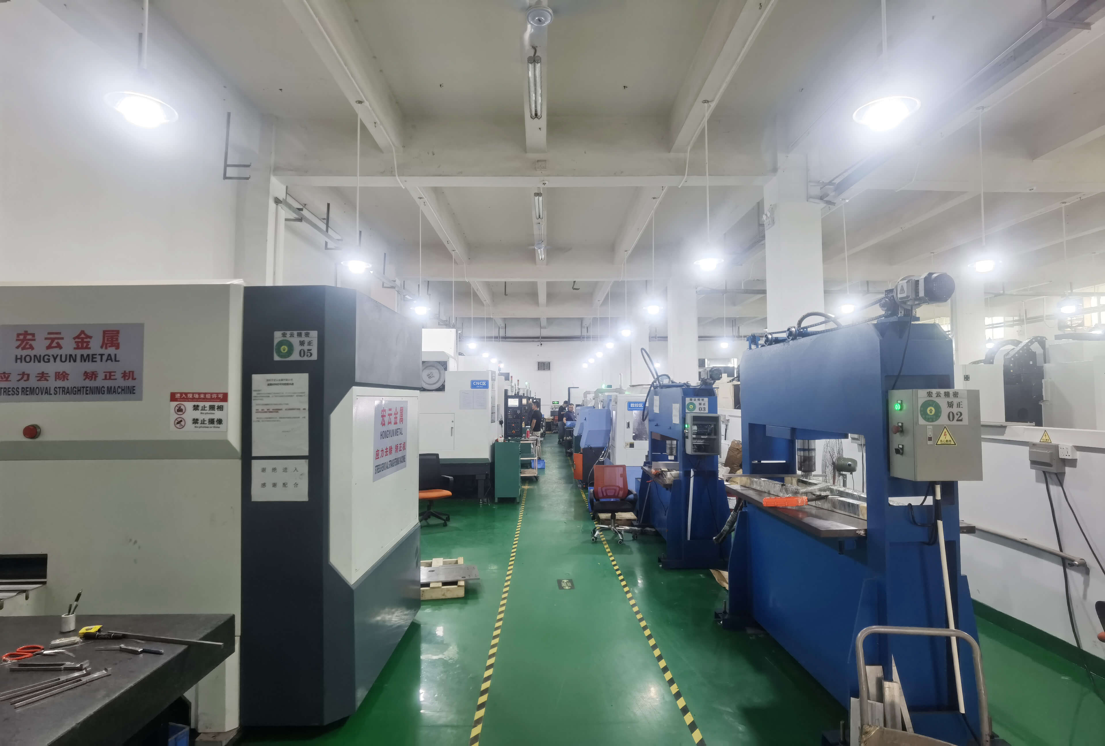
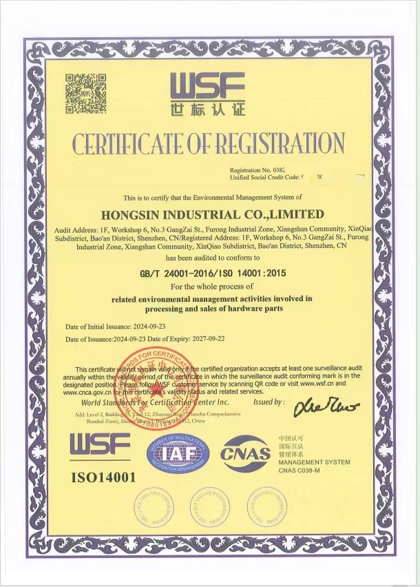
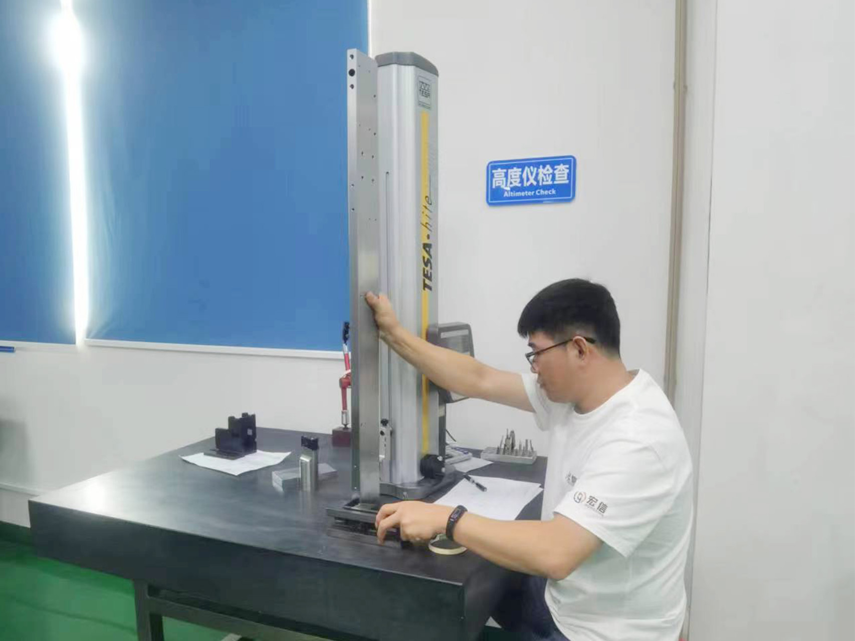
Comprehensive Quality Control: Equipped with Zeiss CMMs (Coordinate Measuring Machines) and optical measurement instruments to ensure the dimensional accuracy and positional integrity of every complex feature and geometric dimension.
Vacuum & Cleanliness Processing: We provide surface treatments optimized for vacuum environments, as well as cleaning and packaging services that meet strict cleanroom standards.
From Prototyping to Mass Production: Whether you require a novel substrate prototype for the R&D phase or a stable supply for mass production, we are fully capable of meeting your needs.












Recommend Products
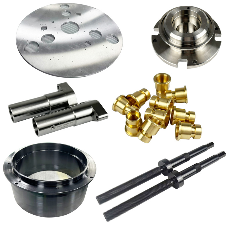
 Providing precision engineering machining services including CNC turning and milling services, CNC lathe components. cnc turning service
 Precision CNC parts for motorcycles and automotive machinery.
 CNC Machining Services in China for High Precision Parts
 Specializing in precision CNC machining for plastic components and tool steel.